Solution Found!
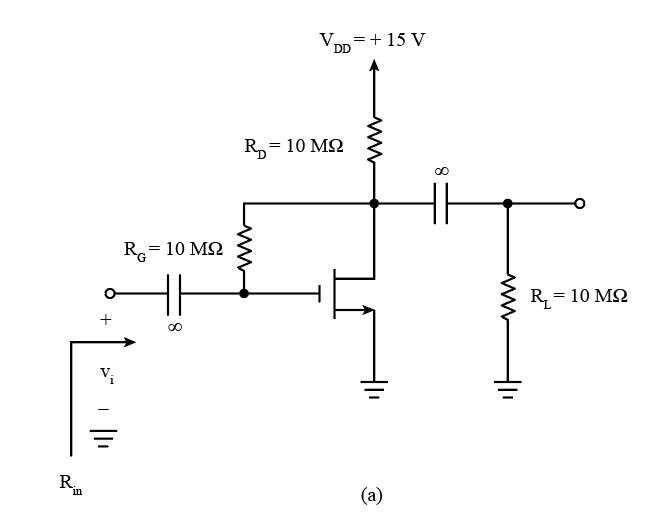
Consider the amplifier circuit of Fig. 7.15(a) without the load resistance RL and with
Chapter 7, Problem 7.4(choose chapter or problem)
Consider the amplifier circuit of Fig. 7.15(a) without the load resistance RL and with channel-length modulation neglected. Let VDD = 5 V, Vt = 0.7 V, and kn = 1 mA/V2 . Find VOV , ID, RD, and RG to obtain a voltage gain of 25 V/V and an input resistance of 0.5 M . What is the maximum allowable input signal, vi ?
Questions & Answers
QUESTION:
Consider the amplifier circuit of Fig. 7.15(a) without the load resistance RL and with channel-length modulation neglected. Let VDD = 5 V, Vt = 0.7 V, and kn = 1 mA/V2 . Find VOV , ID, RD, and RG to obtain a voltage gain of 25 V/V and an input resistance of 0.5 M . What is the maximum allowable input signal, vi ?
ANSWER:Problem 7.4
Consider the amplifier circuit of Fig. 7.15(a) without the load resistance


Step by Step Solution
Step 1 of 5
Consider the DC equivalent circuit shown in figure below.
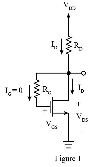
Neglect the load resistance and the resistance 
